
 FEATURED
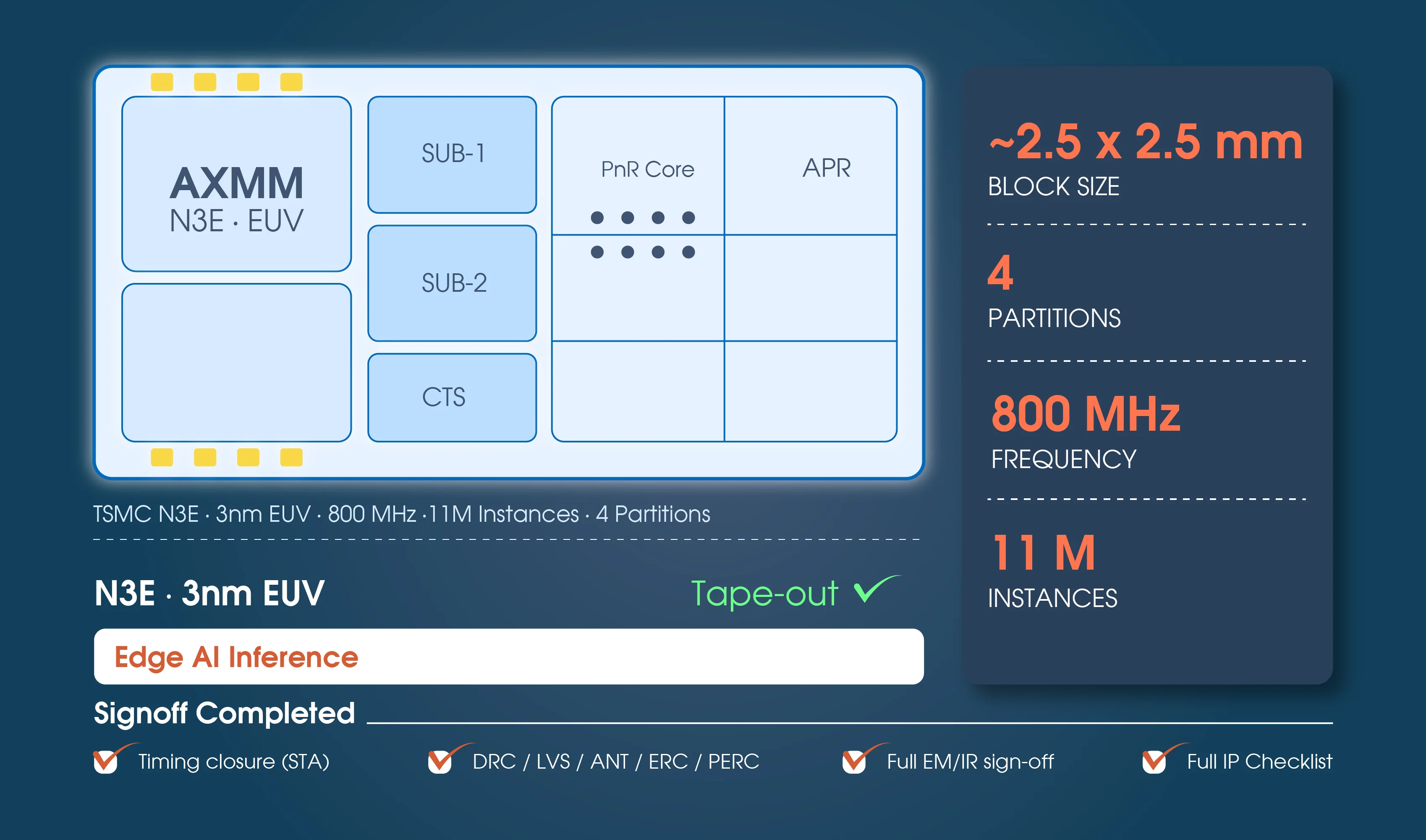
Hierarchical APR on TSMC N3E — AXMM top-block
4-partition hierarchical PnR for an edge AI inference processor. IOPin budgeting, cross-partition routing congestion resolution, ELVT leakage containment, EUV multi-patterning DRC/DFM compliance, and MCMM STA sign-off on schedule.
 FEATURED
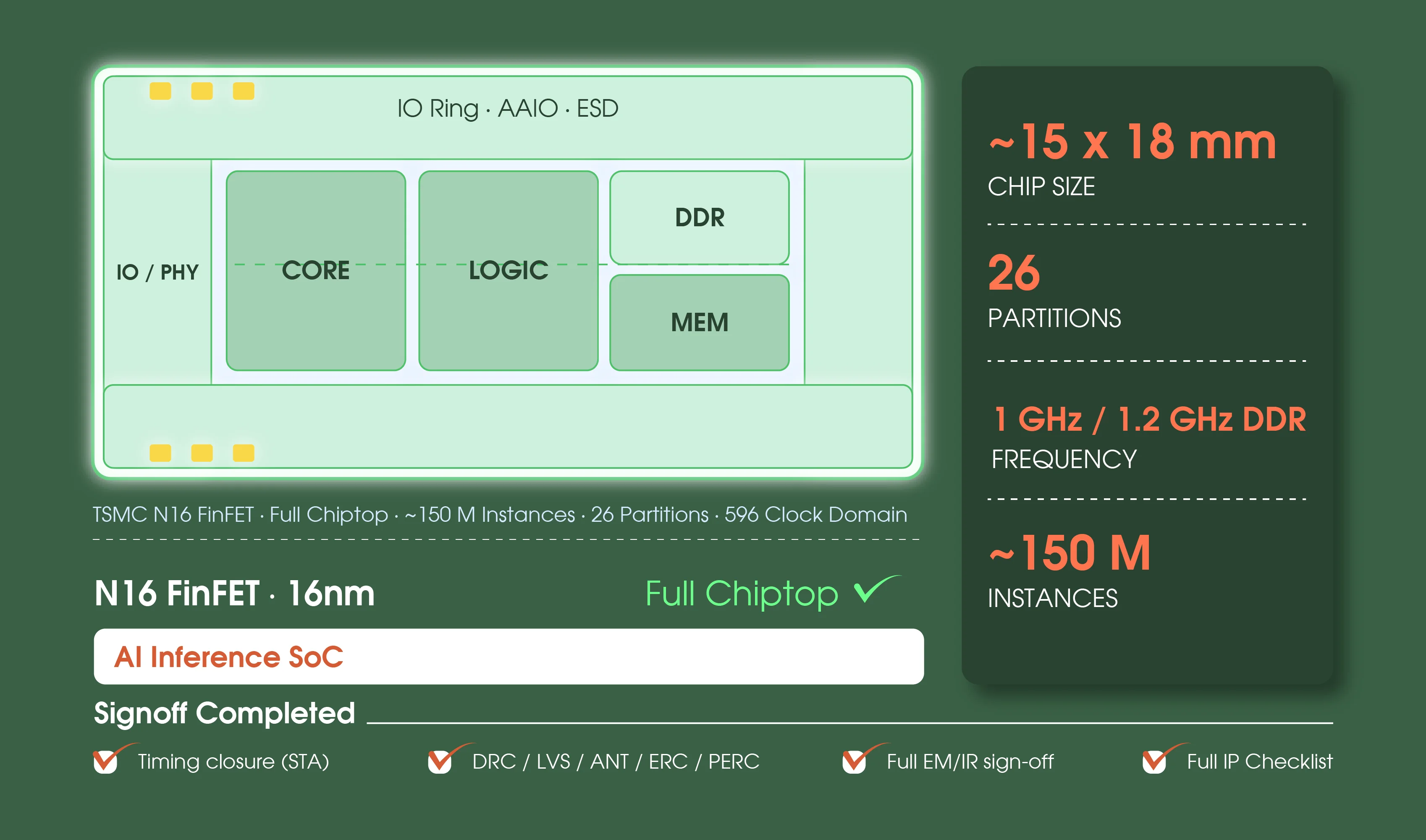
RTL-to-GDSII full-chip — 150M instances
Turnkey hierarchical PnR for an AI inference SoC across 26 partitions, 8 hardened IPs, 596 clock domains. MCMM/POCV STA sign-off, EM-IR closure, custom PG mesh routing, full-chip DRC/LVS/ERC/ANT sign-off.
 FEATURED
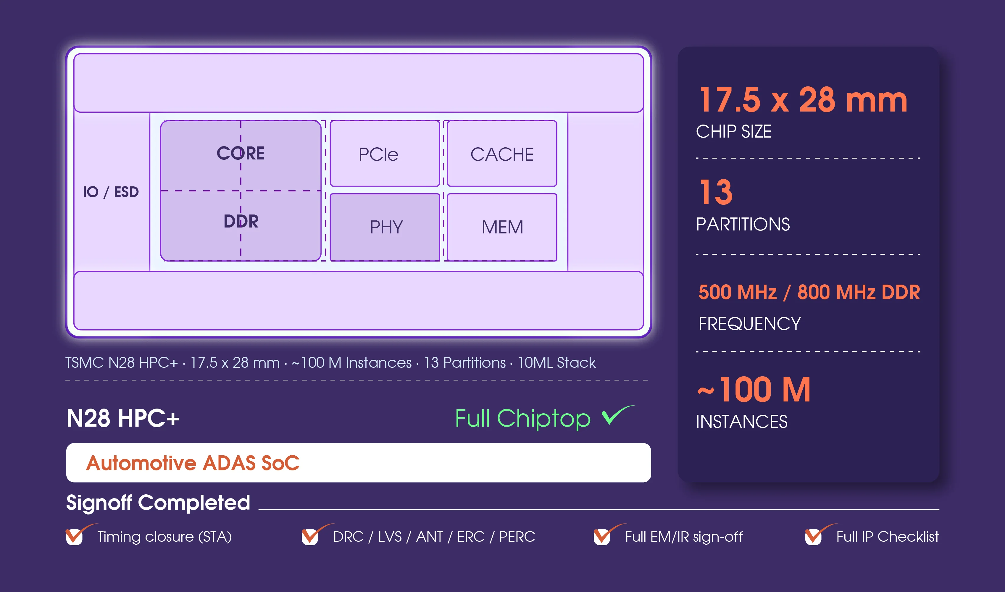
Largest-die RTL-to-GDSII — 17.5 x 28 mm
Turnkey full-chip PnR for an Automotive ADAS vision SoC. 13 partitions, 396 clock domains, 10LM5X2Y2ZUTRDL stack. AOCV MCMM STA sign-off, EM-IR closure, full DRC/LVS/ERC/ANT/ICOVL/TCD sign-off.
 FEATURED
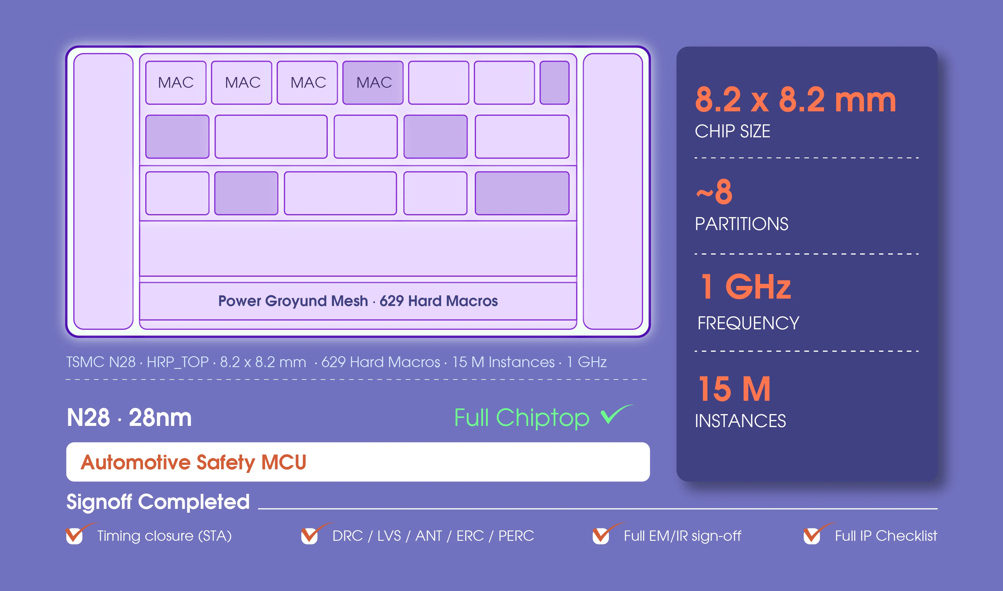
High-density full-chip — HRP_TOP, 629 hard macros
Full chiptop for an Automotive safety MCU on M1-M9 stack, 629 hard macros. AC timing and internal/interface STA sign-off at 1 GHz under narrow-channel routing congestion. Full DRC/LVS/ERC/PERC sign-off.
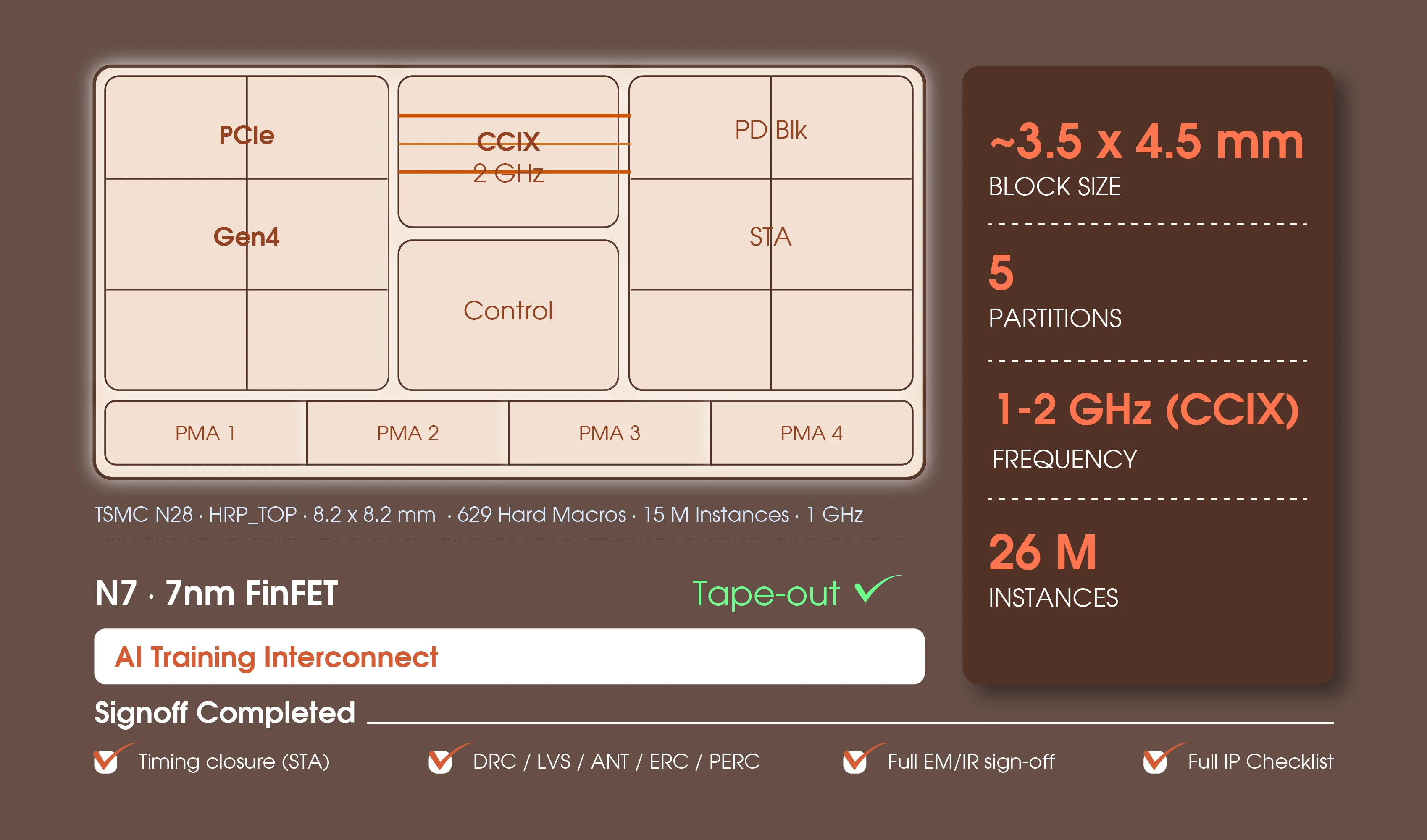
PCIe Gen4 / CCIX top-block — 2 GHz timing closure
CCIX cache-coherent interconnect for AI training accelerators. Multi-source CTS across 388+412 clock domains, AOCV STA sign-off on CCIX link, 4 SerDes PMA custom routes with NDR, and full DRC/DFM sign-off.
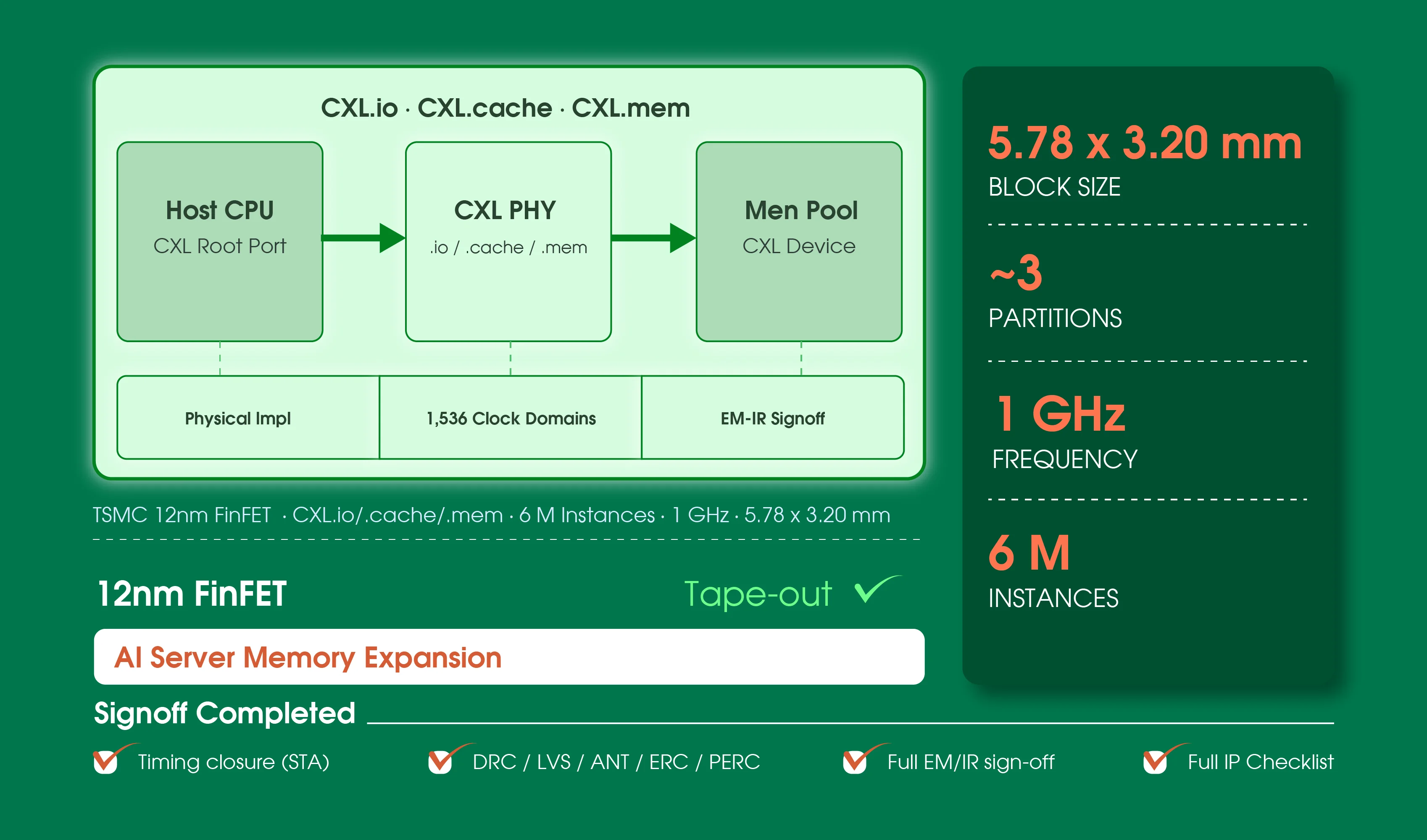
CXL.io / .cache / .mem interconnect block
CXL protocol stack enabling AI server memory coherency and pooling. 1,536 clock domains, IP-boundary STA sign-off, EM-IR closure, post-layout parasitic extraction for STA. Full DRC/LVS sign-off.
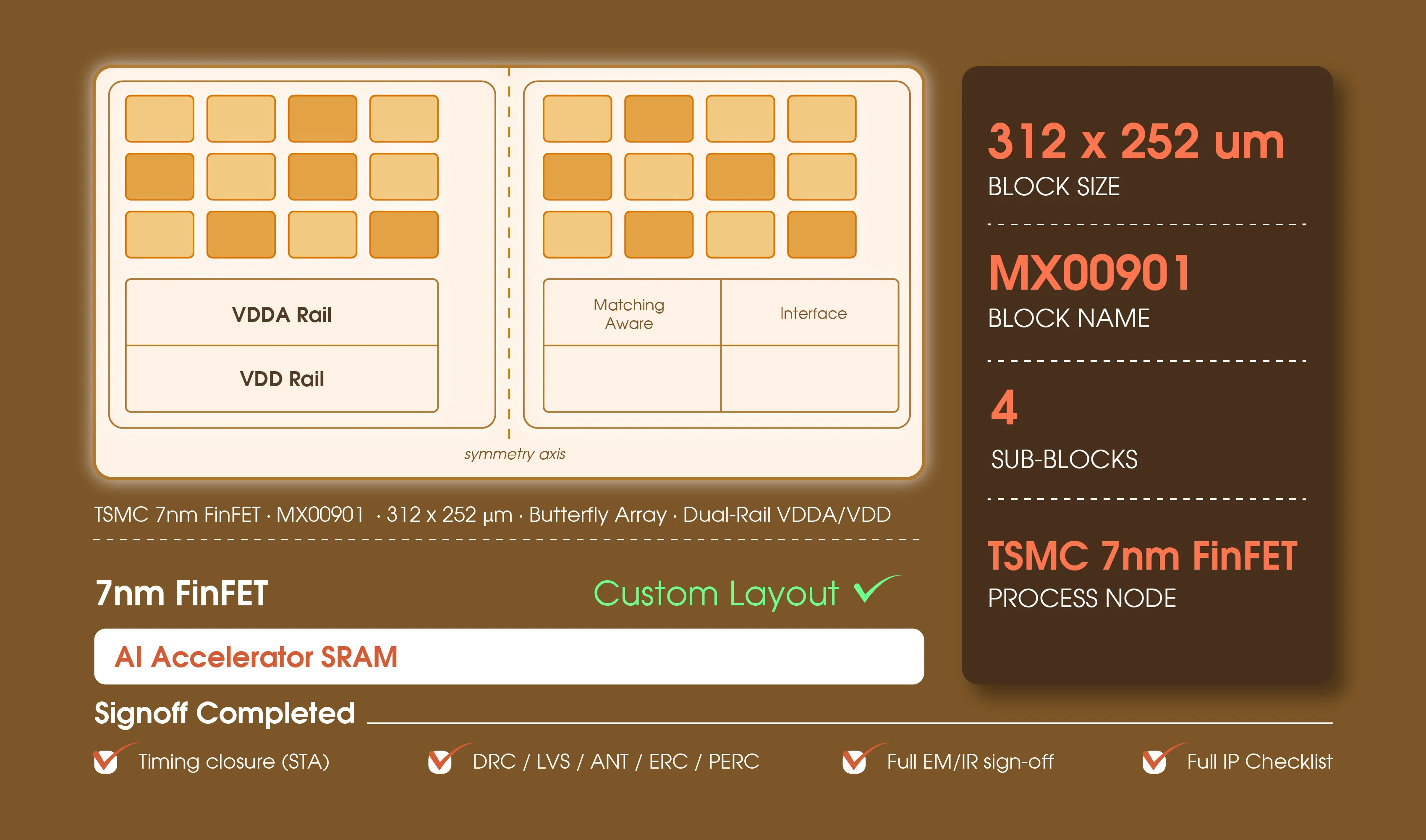
Butterfly memory array — MX00901
Full-custom SRAM bitcell array for AI accelerator on-chip memory. Butterfly architecture with matching-aware placement, parasitic-optimized feed-through routing, and dual-rail VDDA/VDD. DRC/LVS/ERC sign-off.
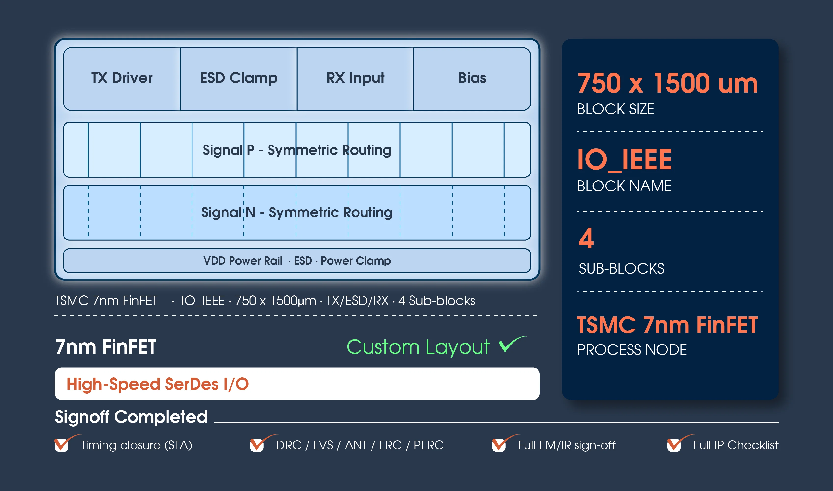
IEEE-standard I/O pad — IO_IEEE
High-speed I/O pad for PCIe/SerDes interfaces. Full-custom layout with TX driver, ESD protection, RX input buffer, and power clamp. Symmetric critical-signal routing and full DRC/LVS/ICV sign-off.
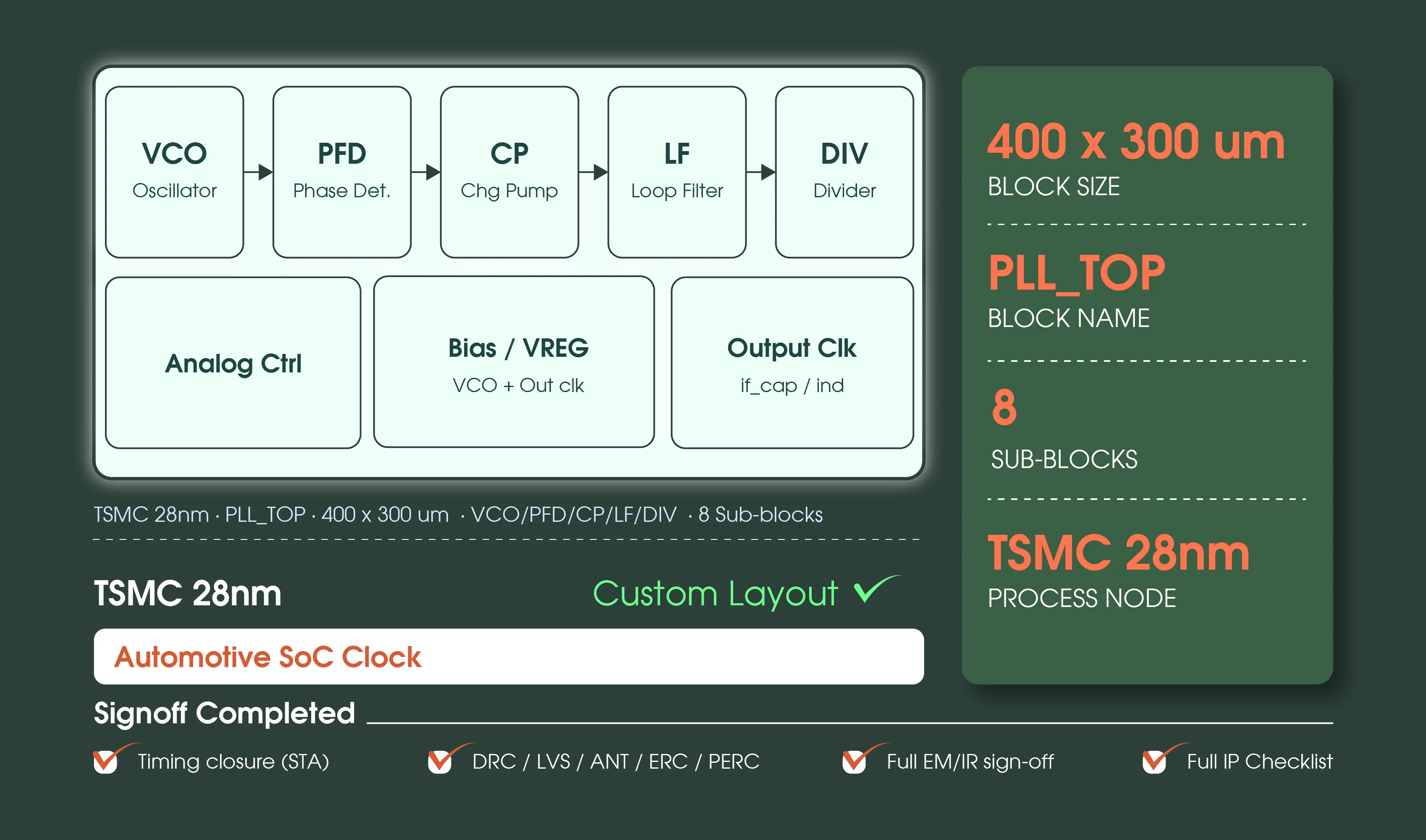
Full-custom PLL — PLL_TOP
Analog PLL for Automotive and communications SoC clock generation. VCO, charge pump, loop filter capacitor/resistor, phase-frequency detector, output divider, and digital control. Matching-aware placement and VREG grid for VCO and output clocks.
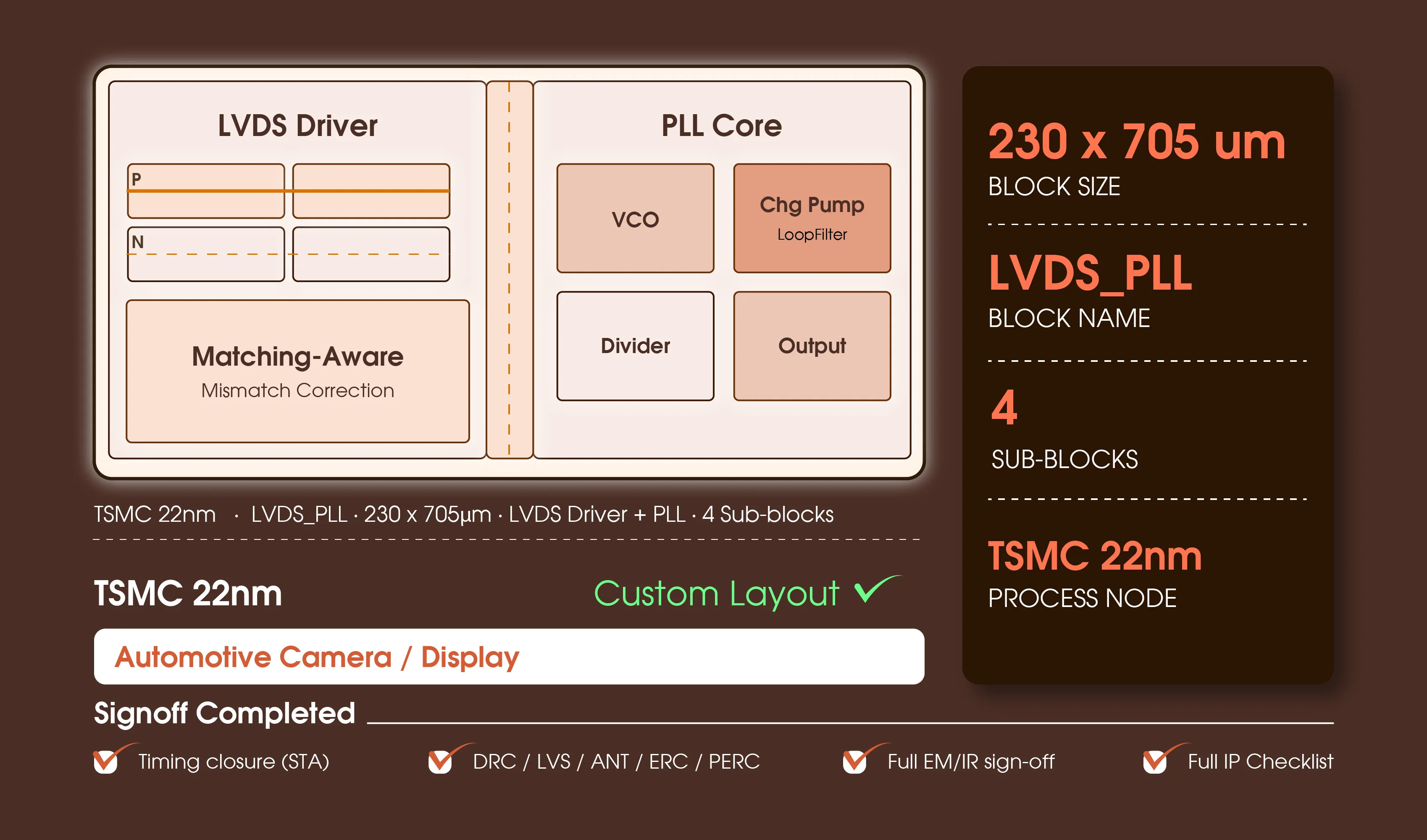
LVDS interface with PLL — LVDS_PLL
Low-voltage differential signaling with integrated PLL for Automotive camera serial link and display interface. Differential P/N matching placement, symmetric critical-path routing, and mismatch-corrected device pairs.